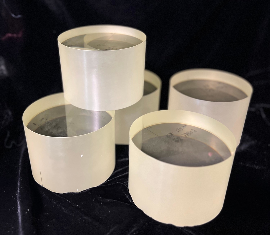
• LiNbO3 Wafers The Ultimate Choice for Cutting-Edge Technologies and Optoelectronic Applications
LiNbO3 Wafers The Ultimate Choice for Cutting-Edge Technologies and Optoelectronic Applications

LiNbO3 Wafers The Ultimate Choice for Cutting-Edge Technologies and Optoelectronic Applications

商品の詳細:

起源の場所: 中国
ブランド名: CQT
証明: ISO:9001, ISO:14001
モデル番号: ニオブ酸リチウムウェーハ

お支払配送条件:

最小注文数量: 10個のPC
価格: 交渉可能
パッケージの詳細: 真空密封カセット瓶のパッケージ
受渡し時間: 1〜4週間
支払条件: T/T
供給の能力: 10000 PCS/月
ベストプライス 連絡先

詳細情報

製品: ニオブ酸リチウムウェーハ キャラクター: SAW,光学グレード
直径: 3インチ,4インチ,6インチ,8インチなど オリエンテーション: X,Y,Z,64Y,128Yなど
厚さ: 0.35mm,0.50mm,1.00mm TTV: <10um>
表面の粗さ: ra <0.5nm ra <1nm アプリケーション: 光学導波管およびMicrowaveguides

製品の説明

LiNbO3 Wafers The Ultimate Choice for Cutting-Edge Technologies and Optoelectronic Applications


Elevate your photonics and telecommunications innovations with our high-purity Lithium Niobate (LiNbO₃) wafers, engineered for unmatched optical and electro-optical excellence. Renowned for its exceptional nonlinear optical properties, high electro-optic coefficient, and wide transparency range (350–5000 nm), LiNbO₃ is the cornerstone material for cutting-edge applications in modulators, frequency converters, and acousto-optic devices.

Our wafers are meticulously crafted using advanced Czochralski crystal growth technology, ensuring ultra-low defect density, uniform thickness, and precise orientation (Z-cut/X-cut). With superior surface polish and minimal birefringence, they deliver unparalleled signal integrity and conversion efficiency, ideal for high-speed optical communication, quantum computing, and laser systems.

Customizable to meet your specifications—including diameter, thickness, and doping options—our LiNbO₃ wafers empower researchers and engineers to push boundaries in next-gen technologies. Backed by rigorous quality control and global technical support, we guarantee reliability and performance.

Choose excellence. Choose our LiNbO₃ wafers—where precision meets innovation.


LiNbO3 Wafers The Ultimate Choice for Cutting-Edge Technologies and Optoelectronic Applications 0LiNbO3 Wafers The Ultimate Choice for Cutting-Edge Technologies and Optoelectronic Applications 1LiNbO3 Wafers The Ultimate Choice for Cutting-Edge Technologies and Optoelectronic Applications 2

LiNbO3 Wafers The Ultimate Choice for Cutting-Edge Technologies and Optoelectronic Applications 3

LiNbO3 Wafers The Ultimate Choice for Cutting-Edge Technologies and Optoelectronic Applications 4


LiNbO3 Wafers The Ultimate Choice for Cutting-Edge Technologies and Optoelectronic Applications 5


LiNbO3 Wafers The Ultimate Choice for Cutting-Edge Technologies and Optoelectronic Applications 6


FAQs:


  1. Q: What are the products you mainly work on?

A: We look at ourselves as the piezo wafer specialist. We are the very first to work with Single Crystal Quartz in China about 30 years ago. Then gradually we step in the field of LiNbO3, LiTaO3, Quartz glass, LGS, CTGS etc. Especially, if you are looking for a piezo quartz supplier, we are the ultimate choice! We export millions of quartz blanks each year because we master the AT, SC and IT cuts with superior angle precision.


  1. Q: Can you accept product customization?

A: Yes, of course. We can fabricate as per your request. In addition, we are so experienced with piezo wafers that we can provide you relevant suggestions if you are not 100% sure about your choice. Besides, we do have some standard wafers in stock, please check with us.


  1. Q: Can you deliver the goods via our courier agent?

A: Yes, we would suggest you go with the courier agent you are most familiar with (DHL, FedEX, UPS etc.). We can ship via your account. And, of course, we will pack the products safely in acceptable size to help you save the shipping cost. If you need us to take care of the freight, it’s also not a problem. We also have good discount with the international courier companies.


  1. Q: How can you guarantee we get what we want safely?

A: The wafer products are fragile and sometimes expensive. The last thing, as the manufacturer, we want to see is the products we make were damaged during courier. As a result, we will pack the wafers adequately and put them in a proper carton filled with buffer sponge. However, accidents are inevitable sometimes. So, please follow the “Acceptance check” steps shown in the drawings below. If the unwanted happened, we will either give the replenishment or refund if you follow the checking steps.


Acceptance Check

LiNbO3 Wafers The Ultimate Choice for Cutting-Edge Technologies and Optoelectronic Applications 7


  • The product is fragile. We have adequately packed it and labeled it fragile. We deliver through excellent domestic and international express companies to ensure transportation quality.


  • After receiving the goods, please handle with care and check whether the outer carton is in good condition. Carefully open the outer carton and check whether the packing boxes are in alignment. Take a picture before you take them out.

  • Please open the vacuum package in a clean room when the products are to be applied.


  • If the products are found damaged during courier, please take a picture or record a video immediately. DO NOT take the damaged products out of the packaging box! Contact us immediately and we will solve the problem well.

この製品の詳細を知りたい
に興味があります LiNbO3 Wafers The Ultimate Choice for Cutting-Edge Technologies and Optoelectronic Applications タイプ、サイズ、数量、素材などの詳細を送っていただけませんか。
ありがとう!
お返事を待って。